


Triple Quantum Breakthrough: Infrastructure, Integration & Industry Validation Signal Computing Maturation
🎯 TL;DR – Three Simultaneous Quantum Milestones
- Infrastructure Build-Out: Chicago’s 128-acre Illinois Quantum and Microelectronics Park (IQMP) begins phase one construction with PsiQuantum as anchor tenant—2027 completion target
- Technology Miniaturization: Germany’s SmaraQ consortium integrates UV photonic waveguides directly onto ion-trap quantum chips, replacing room-sized optical systems
- Industry Validation: DARPA advances 11 companies to Stage B of Quantum Benchmarking Initiative, rigorously evaluating paths to utility-scale quantum computing by 2033
- Combined Signal: These developments represent quantum computing’s transition from research novelty to engineered infrastructure, manufacturable hardware, and standardized benchmarking
Rendering of the Illinois Quantum and Microelectronics Park at the former U.S. Steel South Works site in Chicago
November 2025 marks a pivotal moment in Quantum AI computing’s evolution: three simultaneous developments across infrastructure, chip integration, and industry validation demonstrate the field’s maturation from laboratory curiosity to engineered industrial reality. While previous breakthroughs focused on qubit count and error correction milestones, this week’s announcements address the practical requirements for deploying quantum computers at scale—purpose-built facilities, miniaturized control systems, and standardized performance metrics.
The convergence is not coincidental. As quantum systems grow from dozens to thousands of qubits, they demand specialized infrastructure (cryogenic cooling plants spanning acres), manufacturable photonic components (replacing bulky free-space optics with lithographic waveguides), and rigorous third-party verification (DARPA’s independent validation teams). Together, these developments suggest quantum computing is entering its “industrial revolution” phase.
🏗️ Infrastructure: Chicago’s Quantum Campus Breaks Ground

PsiQuantum announces groundbreaking on America’s largest quantum computing facility in Chicago
From Steel Mill to Silicon: The IQMP Transformation
The Illinois Quantum and Microelectronics Park (IQMP) represents the first purpose-built quantum computing campus in the United States. Located at the decommissioned U.S. Steel South Works site—once the world’s largest steel foundry—the 128-acre development transforms industrial heritage into quantum infrastructure. Related Midwest and Clayton Real Estate Group recently acquired the land, with phase one construction now underway on approximately 30 acres.
PsiQuantum’s Photonic Anchor
PsiQuantum, the park’s anchor tenant, is developing fault-tolerant quantum computers based on photonic qubits—particles of light manipulated at cryogenic temperatures. Unlike superconducting or trapped-ion systems that require ultra-high vacuum chambers, photonic architectures promise room-temperature operation for control electronics (though the photon detectors still need deep cooling). The company’s silicon photonics approach leverages existing semiconductor manufacturing infrastructure, potentially enabling mass production.
The IQMP facility will house:
- Cryogenic cooling plant: Industrial-scale dilution refrigerators maintaining millikelvin temperatures across multiple quantum processors
- Equipment labs: Clean rooms for photonic chip assembly and testing
- Research collaboration spaces: Shared facilities for universities and private companies to access quantum hardware
- Office and manufacturing areas: Co-locating R&D with production to accelerate iteration cycles
Timeline and Economic Impact
Phase one targets 2027 completion, with subsequent phases expanding across the full 128-acre site through the early 2030s. The development aims to establish Illinois as a quantum computing hub rivaling initiatives in Boulder, Colorado (home to NIST and multiple quantum startups) and the San Francisco Bay Area. Cook County approved $20 million in investment support, recognizing potential for high-skill job creation and technology sector diversification.
🔬 Technology: Germany’s SmaraQ Miniaturizes Quantum Optics
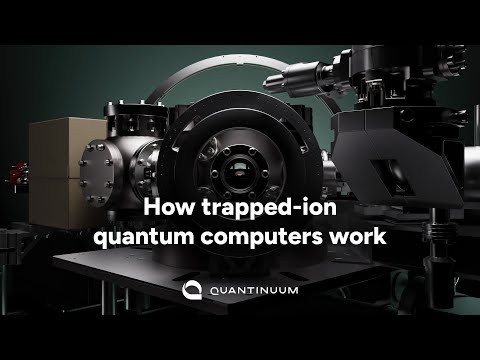
How trapped-ion quantum computers work—understanding the technology behind SmaraQ’s photonic integration
The Ion-Trap Scaling Challenge
Ion-trap quantum computers use naturally identical charged atoms (ions) as qubits, offering exceptional coherence times and gate fidelities. Companies like IonQ and Quantinuum have demonstrated systems with 32+ qubits achieving >99.9% two-qubit gate fidelity. However, scaling beyond hundreds of qubits hits a fundamental bottleneck: optical access.
Current ion-trap systems require:
- Individual laser beams for each ion (initialization, gate operations, readout)
- Free-space optical systems with hundreds of mirrors, lenses, and beam splitters
- Vibration isolation tables occupying entire laboratory rooms
- Manual alignment procedures taking days or weeks
This complexity limits maximum processor size and prevents the millions of qubits required for useful quantum algorithms. SmaraQ addresses this through on-chip photonic integration.
Aluminum Nitride Waveguides: Nanometer-Scale Light Control
The SmaraQ consortium—QUDORA Technologies, AMO GmbH, and Fraunhofer IAF—is developing ultraviolet (UV) photonic components integrated directly onto ion-trap chips. The approach uses two key materials:
These waveguides, fabricated through lithography (the same technique used for computer chips), are ten thousand times thinner than a human hair yet deliver UV light with nanometer precision. By integrating them onto the same chip holding trapped ions, SmaraQ eliminates bulky external optics.
Supply Chain Sovereignty
Beyond technical advantages, SmaraQ aims to establish a Germany-based supply chain for quantum photonics—part of the European Union’s broader strategy for technological sovereignty. The project receives funding from Germany’s Federal Ministry of Research, Technology, and Space (BMFTR) through 2028, aligning with the EU Chips Act’s emphasis on advanced semiconductor capabilities.
“On-chip integration represents the path forward for ion-trap quantum computing. We are engineering waveguide structures at the nanometer scale that deliver light with pinpoint precision exactly where our ion qubits demand it.” — Dr. Maik Scheller, Head of Photonics at QUDORA
Implications for Scaling
If successful, SmaraQ’s approach enables:
- Thousands of qubits per chip: Dense waveguide arrays controlling each ion individually
- Automated assembly: Lithographic fabrication replaces manual optical alignment
- Reduced footprint: Room-sized optical tables shrink to chip-scale components
- Lower cost: Semiconductor manufacturing economics versus custom optics
✅ Validation: DARPA’s Rigorous Benchmarking Narrows the Field

DARPA’s Quantum Benchmarking Initiative overview—from concept to independent validation
From Hype to Hard Metrics
The quantum computing field has long suffered from conflicting performance claims and non-standardized benchmarks. DARPA’s Quantum Benchmarking Initiative (QBI) addresses this through independent third-party verification. On November 6, 2025, DARPA advanced 11 companies to Stage B—a year-long technical validation phase assessing whether their quantum computer concepts can realistically achieve utility-scale operation by 2033.
The Three-Stage Gauntlet
QBI operates in three phases:
- Stage A (Completed): Companies presented conceptual architectures demonstrating a plausible path to utility-scale quantum computing. Approximately 20 companies entered; 11 advanced.
- Stage B (Current, ~1 year): DARPA evaluates detailed R&D plans, risk-mitigation strategies, prototype roadmaps, and manufacturing pathways. Government teams assess whether designs can be constructed and operated as proposed.
- Stage C (Future): Independent verification and validation teams test actual hardware against standardized benchmarks, providing authoritative performance data.
The 11 Selected Companies
DARPA’s Stage B performers represent diverse qubit modalities, each with distinct advantages and challenges:
| Company | Location | Qubit Technology | Key Strength |
|---|---|---|---|
| Atom Computing | Boulder, CO | Neutral Atoms | Scalable arrays, long coherence times |
| Diraq | Sydney, Australia | Silicon CMOS Spin Qubits | Semiconductor manufacturing compatibility |
| IBM | Yorktown Heights, NY | Superconducting Qubits | Modular processors, error correction roadmap |
| IonQ | College Park, MD | Trapped Ions | High-fidelity gates, all-to-all connectivity |
| Nord Quantique | Sherbrooke, Canada | Superconducting + Bosonic Error Correction | Hardware-efficient error correction |
| Photonic Inc. | Vancouver, Canada | Optically-Linked Silicon Spin Qubits | Telecom-band photonic interconnects |
| Quantinuum | Broomfield, CO | Trapped-Ion QCCD Architecture | Highest demonstrated quantum volume |
| Quantum Motion | London, UK | MOS Silicon Spin Qubits | CMOS foundry integration |
| QuEra Computing | Boston, MA | Neutral Atoms | Large-scale arrays (256+ atoms) |
| Silicon Quantum Computing | Sydney, Australia | Precision Atom Qubits in Silicon | Atomic-scale fabrication precision |
| Xanadu | Toronto, Canada | Photonic Quantum Computing | Room-temperature operation (control layer) |
What Stage B Entails
Over the next year, Stage B performers must provide:
- Detailed engineering plans: Component specifications, fabrication processes, assembly procedures
- Prototype burn-down schedules: Milestones demonstrating progress toward full-scale systems
- Risk mitigation strategies: Identification of potential failure modes and contingency plans
- Manufacturing pathways: Transition from hand-assembled prototypes to reproducible production
DARPA’s evaluation teams—combining government experts and independent reviewers—will assess whether each performer’s roadmap is credible or overly optimistic. Only those passing rigorous technical scrutiny advance to Stage C hardware testing.
“The move from conceptual review to rigorous validation suggests DARPA is narrowing focus from ‘could this work’ to ‘can this be built.'” — The Quantum Insider
🔗 The Convergence: What These Three Developments Mean Together
From Lab Demos to Industrial Infrastructure
Viewed in isolation, each announcement represents incremental progress. Viewed together, they signal quantum computing’s transition from academic research to industrial deployment:
Timelines Align Around 2027-2033
The convergence extends to project timelines:
- 2027: IQMP phase one operational, SmaraQ completes development (project funded through 2028)
- 2028-2030: DARPA Stage C validation of select performers
- 2033: DARPA’s target date for utility-scale quantum computing achieving computational value exceeding cost
This 6-8 year horizon suggests industry consensus around a realistic deployment schedule—neither the “quantum computers next year” hype of 2019 nor the “decades away” pessimism of skeptics.
Geographic Distribution: Quantum Hubs Emerge
The three announcements also reveal emerging quantum computing clusters:
- North America: Chicago (IQMP), Colorado (Quantinuum, Atom Computing), Maryland (IonQ), Boston (QuEra), Canada (Xanadu, Nord Quantique, Photonic Inc.)
- Europe: Germany (SmaraQ consortium), UK (Quantum Motion)
- Asia-Pacific: Australia (Diraq, Silicon Quantum Computing)
Geopolitical competition in quantum technology now manifests through infrastructure investments (Chicago IQMP), industrial policy (Germany’s BMFTR funding), and government validation programs (DARPA QBI). Quantum computing has become a strategic technology requiring national ecosystems, not just brilliant researchers.
🚀 Bottom Line
November 2025’s triple announcement—Chicago’s quantum campus, Germany’s on-chip photonics, and DARPA’s technical validation—collectively demonstrates quantum computing’s maturation beyond laboratory prototypes. The field now requires industrial infrastructure, manufacturable components, and standardized benchmarks. While significant technical challenges remain (error correction, qubit scaling, algorithm development), the investment in physical facilities, supply chains, and validation processes suggests stakeholders believe utility-scale quantum computing is achievable within the 2027-2033 timeframe.
The quantum revolution is no longer a matter of “if” but “how soon” and “through which architectures.”
🤖 AI-Powered Quantum Insights: Prompts for Deeper Exploration
“Compare the capital expenditure requirements for building a 128-acre quantum computing facility like IQMP versus an equivalent-sized semiconductor fab or hyperscale data center. What are the unique cost drivers for quantum infrastructure (cryogenic systems, vibration isolation, clean rooms)?”
“Evaluate the technical challenges of integrating UV aluminum nitride waveguides onto ion-trap chips. What are the material science constraints (thermal expansion mismatch, optical loss at UV wavelengths, fabrication defects) and how do they compare to visible/IR photonic integration?”
“Design a rigorous benchmarking protocol for comparing quantum computers with different qubit modalities (superconducting, trapped ion, neutral atom, photonic). What metrics should be standardized (gate fidelity, coherence time, error rates, quantum volume, algorithmic qubits) and how do you account for architectural differences?”
“Analyze the strategic implications of quantum computing infrastructure being concentrated in the US, Germany, and Australia. What are the technology sovereignty risks if critical photonic components or cryogenic systems have single-source suppliers? How might export controls affect the field?”
“Assess whether DARPA’s 2033 target for utility-scale quantum computing is realistic. What are the remaining technical barriers (error correction overhead, qubit interconnects, algorithm development), and which applications are most likely to achieve ‘computational value exceeding cost’ first?”
❓ Frequently Asked Questions
🔗 Sources and Further Reading
- The Quantum Insider: Phase One Construction Begins on Chicago Quantum Computing Facility
- PsiQuantum: Breaks Ground on America’s Largest Quantum Computing Project
- University of Chicago: Groundbreaking of IQMP Creates Anchor for Quantum Innovation
- The Quantum Insider: SmaraQ Integrates Quantum Optics on a Chip
- Fraunhofer IAF: SmaraQ Integrates Quantum Optics on a Chip
- QUDORA: SmaraQ Paves the Way for Next-Generation Quantum Computers
- DARPA: Quantum Benchmarking Initiative (QBI)
- The Quantum Insider: DARPA Advances Quantum Computing Initiative
- Quantum Computing Report: DARPA’s QBI Advances with Eleven Teams Moving to Stage B
- IonQ: Advances to Stage B of DARPA’s Quantum Benchmarking Initiative
- Quantinuum: Selected by DARPA to Advance to Stage B of QBI

Kristof GeorgeAI Strategist, Fintech Consultant & Publisher of QuantumAI.co
Kristof George is a seasoned digital strategist and fintech publisher with over a decade of experience at the intersection of artificial intelligence, algorithmic trading, and online financial education. As the driving force behind QuantumAI.co, Kristof has curated and published hundreds of expert-reviewed articles exploring the rise of quantum-enhanced trading, AI-based market prediction systems, and next-gen investment platforms.
Why Trust Kristof George?
✅ Experience: 10+ years in fintech publishing, affiliate compliance, and AI content development.
🧠 Expertise: Deep knowledge of algorithmic trading platforms, quantum computing trends, and the evolving regulatory landscape.
🔍 Authoritativeness: Cited across industry blogs, crypto review networks, and independent watchdog forums.
🛡 Trustworthiness: Committed to fact-checking, scam exposure, and promoting ethical AI adoption in finance.
